NPN Transistor Troubleshooting: A Practical Guide for Circuit Debug and Component Reliability
Master NPN transistor troubleshooting with this practical guide for electronics engineers and component buyers. Learn to spot subtle failure signatures, interpret datasheet parameters like VBE, hFE, and SOA, compare NPN vs. PNP debug strategies, and apply in-circuit checks that prevent costly rework. Includes real-world failure analysis insights and actionable answers to the most pressing questions from the lab and the procurement desk.
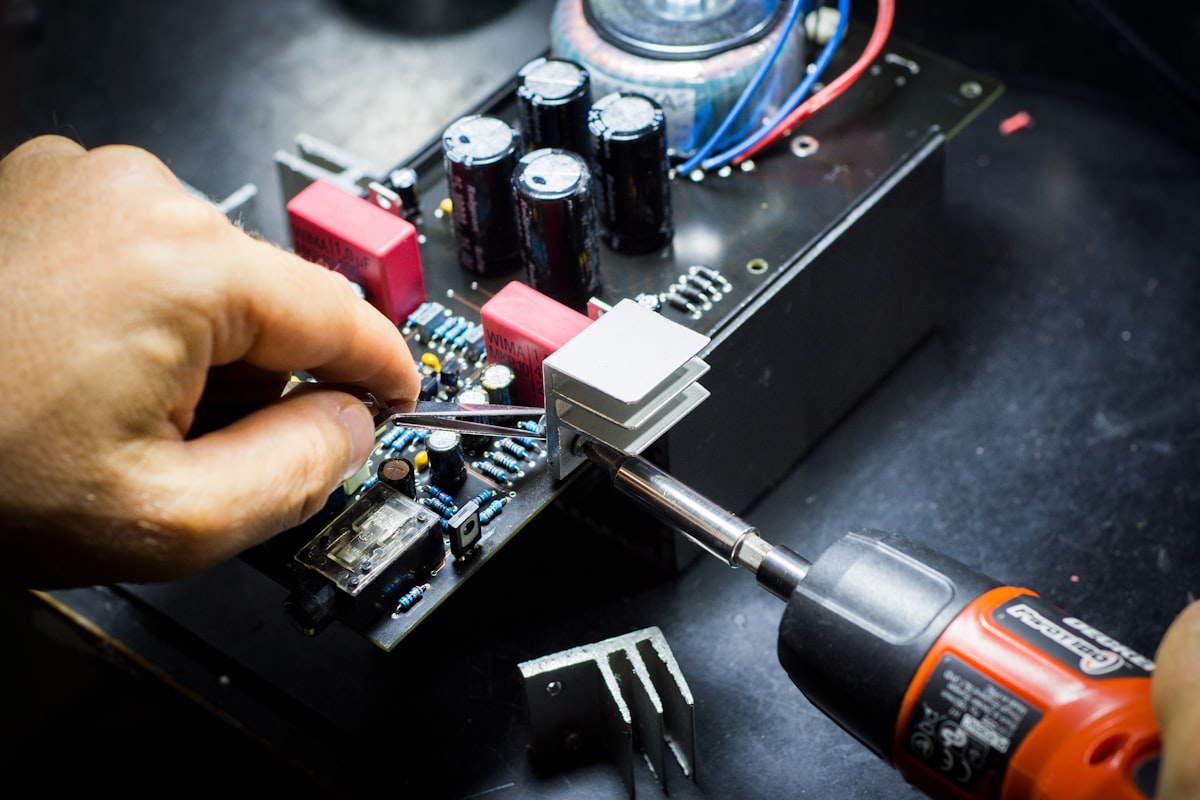
Why NPN Transistor Faults Are More Common Than You Think—and How to Spot Them
When a circuit misbehaves, the humble NPN transistor is rarely the first suspect. After all, semiconductor devices are extremely reliable when operated within their ratings. Yet in the field, NPN transistors fail often enough to keep failure analysis labs busy—and the root cause is rarely a random manufacturing defect. More often, it’s a subtle overstress, a missing flyback diode, or a counterfeit part that slipped through incoming inspection.
Understanding the real failure landscape is the first step toward effective troubleshooting. Gideon Labs notes that NPN transistors are the workhorse switch in most circuits, and their failure modes fall into a few predictable categories: thermal runaway from inadequate heatsinking, secondary breakdown from inductive kickback, and gradual degradation of current gain (hFE) due to prolonged operation near the safe operating area (SOA) boundary. Manufacturing defects do occur—typically in brand-new equipment—but they are rare compared to application-induced failures.
The symptoms you see on the bench can be deceptive. A transistor that measures “good” on a multimeter diode test may still exhibit reduced gain under load, causing erratic switching or low output power. Eureka’s troubleshooting guide emphasizes that for a bipolar junction transistor (BJT), you must check both the base-emitter and base-collector junctions. A healthy NPN shows a forward voltage drop of 0.6–0.7 V from base to emitter and base to collector, while the reverse direction should read open. Any deviation—a short, an open, or a low-resistance leakage path—points to a damaged device.
But in-circuit diagnostics are trickier. Electronics Believer reminds us that parallel components can skew readings, making it essential to compare measurements against a known-good board or to lift one leg of the transistor when in doubt. Ignoring these subtle signs leads to costly rework and field returns. In the following sections, we’ll equip you with the datasheet literacy, comparison strategies, and hands-on checks that turn NPN troubleshooting from guesswork into a systematic process.
Reading the NPN Datasheet Like a Troubleshooter: VBE, hFE, and Safe Operating Area
A datasheet is not just a collection of maximum ratings; it’s a diagnostic roadmap. When a circuit fails, the first place to look is whether the transistor was ever operated within the boundaries set by its manufacturer. Let’s break down the parameters that matter most during debug, using real datasheets from the jellybean C1815 (TO-92 general-purpose), the 2N3055 (power transistor), and the BD239C (medium-power NPN).
| Parameter | Typical Value/Range (Example Parts) | Troubleshooting Significance |
|---|---|---|
| VBE(on) (Base-Emitter Forward Voltage) | 0.6–0.7 V at moderate IC (C1815, BD239C); ~1.5 V max at high current for 2N3055 | If you measure significantly less than 0.5 V or more than 0.9 V in diode mode, the junction is damaged. A low VBE can indicate a leaky or shorted junction. |
| hFE (DC Current Gain) | C1815: 70–700 (grade dependent); 2N3055: 20–70 at 4 A; BD239C: 25–100 at 1 A | A transistor with gain below the minimum datasheet limit may still “work” but will fail to saturate properly, causing overheating. Degraded hFE is a common signature of electrical overstress. |
| VCE(sat) (Collector-Emitter Saturation Voltage) | C1815: 0.25 V max at 100 mA; 2N3055: 1.1 V max at 4 A; BD239C: 0.7 V max at 1 A | Excessive saturation voltage under load means the transistor is not switching fully on, leading to power dissipation and eventual thermal failure. Check base drive current first. |
| IC(max) (Maximum Collector Current) | C1815: 150 mA; 2N3055: 15 A; BD239C: 2 A | Exceeding this rating, even momentarily during inrush or inductive kickback, can cause immediate or latent damage. Always verify with an oscilloscope, not just a multimeter. |
| Ptot (Total Power Dissipation) | C1815: 400 mW (free air); 2N3055: 115 W (case); BD239C: 2 W (free air) | If the transistor case is too hot to touch, you’re likely exceeding the derated power limit. Use a thermal camera to spot hotspots and check heatsink integrity. |
| SOA (Safe Operating Area) | Curves provided in datasheets; secondary breakdown limits apply for power transistors like 2N3055 | Inductive loads can push the operating point outside the SOA even when average power seems low. A missing flyback diode often causes secondary breakdown failure. |
PCB HERO emphasizes that switching characteristics—rise time, fall time, storage time—are just as critical as DC parameters in high-speed circuits. If your NPN is used as a switch and you observe slow edges on the collector waveform, the base drive may be insufficient to sweep carriers out of the base quickly. Always cross-reference the datasheet’s test conditions with your actual circuit: a transistor specified for hFE at VCE = 5 V may behave very differently when you force it into saturation with VCE near 0.2 V.
NPN vs. PNP: Why Your Oscilloscope Probe Placement Changes Everything
When you’re debugging a circuit that mixes NPN and PNP transistors—or when you’re deciding which polarity to use in a new design—the troubleshooting workflow changes dramatically. Arrow Electronics points out that NPN transistors switch faster and are cheaper to manufacture, which is why they dominate high-speed switching and amplifier applications. But PNP transistors offer positive logic alignment that can simplify signal interpretation and make probing more intuitive in certain industrial control systems.
The key difference for debug lies in where you place your oscilloscope ground clip and what voltage levels you expect. With an NPN low-side switch, the emitter is typically grounded, so you can probe the collector relative to ground and see the switching waveform directly. For a PNP high-side switch, the emitter is tied to the positive rail, and the collector swings between the rail and ground; probing the collector requires careful attention to common-mode voltage and isolation. Ersa Electronics notes that insufficient base drive, missing flyback diodes, or floating MCU pins during reset are common pitfalls in both NPN and PNP networks, and they recommend adding pulldown/pullup resistors and a diode to prevent unintended turn-on.
| Comparison Metric | NPN Transistor (Low-Side Switch) | PNP Transistor (High-Side Switch) | Debug Impact & Selection Note |
|---|---|---|---|
| Biasing Configuration | Base positive relative to emitter; emitter grounded | Base negative relative to emitter; emitter tied to V+ | Probing NPN base-emitter is straightforward with a single-ended scope. PNP requires differential probing or careful ground referencing. |
| Switching Speed | Faster (electron mobility advantage) | Slower; hole mobility limits speed | Origin-IC confirms NPNs are preferred for high-speed circuits. If your PNP switch shows sluggish edges, it may be a device limitation, not a fault. |
| Drive Requirements | Current must flow into base; MCU pin sinks to ground to turn off | Current must be pulled out of base; MCU pin sources current to turn off | Floating MCU pins during reset can keep an NPN off (safe) but can turn a PNP on unintentionally. Always use a pullup on NPN base, pulldown on PNP base. |
| Typical Failure Modes | Collector-emitter short from overvoltage; base-emitter open from excessive reverse bias | Similar, but often aggravated by negative transients on the supply rail | In NPN circuits, a short often pulls the output permanently low. In PNP circuits, a short can pull the output high, potentially damaging downstream logic. |
| Probe Placement for Debug | Scope probe on collector, ground clip on emitter/GND | Scope probe on collector, ground clip on V+ (use differential probe if floating) | Misplacing the ground clip can short the supply rail. JLCPCB warns that connecting the wrong sensor type to a mismatched input can create a wiring fault—same caution applies to scope probing. |
In practice, NPN transistors are the default choice for driving relays, motors, and high-current LEDs from Arduino, ESP32, and STM32 boards, as JLCPCB highlights. When you encounter a PNP in such a role, double-check that the base drive circuitry can pull the base low enough to saturate the transistor, especially if the supply voltage is higher than the logic level.
From Breadboard to Production: Practical NPN Circuit Checks That Prevent Rework
Field failures often trace back to a handful of preventable issues that can be caught with a disciplined bench check. The following table summarizes the most frequent NPN circuit problems and the diagnostic steps that reveal them before they escape the lab.
| Symptom | Likely Cause | Diagnostic Test | Solution |
|---|---|---|---|
| Transistor runs hot, output voltage never reaches zero | Insufficient base drive; transistor operating in linear region instead of saturation | Measure VCE under load; compare with datasheet VCE(sat). Check base current: IB should be at least IC/hFE(min) × overdrive factor (2–5). | Reduce base resistor value or increase drive voltage. Verify MCU output can source required current. |
| Collector-emitter short after driving a relay or motor | Missing flyback diode; inductive kickback exceeds VCEO rating | Inspect PCB for a diode across the inductive load (cathode to positive rail for NPN low-side). Scope collector during turn-off for voltage spikes. | Add a fast recovery diode (e.g., 1N4148 for small relays, 1N4007 for larger) directly across the load. Ensure diode rating exceeds supply voltage and peak current. |
| Erratic switching, occasional latch-up | Floating base during MCU reset or power-up; noise coupling | Monitor base voltage during power sequencing. Check for a pulldown resistor from base to ground (10 kΩ typical). | Add a 10 kΩ–100 kΩ pulldown resistor to keep the transistor firmly off when the MCU pin is high impedance. |
| Low gain, device fails under load but passes diode test | Degraded hFE from overstress or counterfeit part | Measure hFE at the operating current using a transistor tester or curve tracer. Compare with datasheet minimum. | Replace with a known genuine part from an authorized distributor. For procurement, implement sample testing of hFE and VCE(sat) on incoming lots. |
| Device fails after prolonged operation, case discolored | Thermal runaway due to inadequate heatsinking or exceeded SOA | Measure case temperature under worst-case load. Check derating curve: power rating drops with ambient temperature. | Improve heatsinking, add a series resistor to limit peak current, or select a transistor with a wider SOA. Use a thermal camera to verify uniform heat distribution. |
Tip: When you suspect a transistor is marginal, swap it with a known-good unit of the same part number. If the circuit behavior changes, the original transistor is likely degraded. This simple A/B test often reveals subtle gain or leakage issues that a basic multimeter check misses.
On the procurement side, incoming inspection should go beyond visual checks. For critical production runs, sample a few transistors from each batch and measure hFE and VCE(sat) at the actual operating current. Counterfeit parts frequently exhibit lower gain and higher saturation voltage, as we’ll discuss in the FAQ. Pair this with a careful review of the datasheet’s SOA curve to ensure your circuit stays well within the safe boundaries, including during startup and fault conditions.
Troubleshooting NPN Transistors: Questions Engineers and Buyers Ask
Q: How can I tell if an NPN transistor is faulty without desoldering it from the board?
Use a multimeter in diode mode to check the base-emitter and base-collector junctions. For an NPN, place the positive lead on the base and the negative lead on the emitter, then on the collector; you should see a forward voltage drop of 0.6–0.7 V. Reverse the leads—both junctions should read open. Next, measure collector-emitter resistance with the base open; it should be very high (megaohms). In-circuit, parallel components can create false readings. If you see a low resistance that doesn’t match the schematic, lift one leg of the transistor or compare against a known-good board. A short between collector and emitter is a definitive sign of failure.
Q: What are the most common failure signatures when driving inductive loads with an NPN transistor?
The classic signature is a collector-emitter short, often caused by the high-voltage spike generated when current through an inductor is interrupted. Without a flyback diode, the collector voltage can soar past the transistor’s VCEO rating, leading to avalanche breakdown and permanent damage. You may also see reduced hFE or thermal runaway if the transistor was repeatedly stressed near its SOA limit. Always scope the collector during switching: a healthy waveform shows a clean pull-down to VCE(sat) and a controlled rise. Excessive ringing or a spike that exceeds the datasheet maximum indicates insufficient protection.
Q: How do counterfeit NPN transistors typically behave in a circuit?
Counterfeit parts often have lower current gain, higher saturation voltage, and inconsistent pinouts. They may work at room temperature with light loads but fail early under rated conditions. Visual clues include irregular markings, poor package finish, and date codes that don’t match the manufacturer’s format. Electrically, measure hFE and VCE(sat) and compare with the genuine datasheet. Procurement teams should source only from authorized distributors and consider sample testing for every new lot. A transistor that costs significantly less than the market price is a red flag.
Q: When should a procurement team reject a batch of NPN transistors based on incoming inspection?
Reject the batch if the measured hFE falls outside the datasheet range for the specified grade, or if VCE(sat) exceeds the maximum limit at the test current. Visual inspection should flag inconsistent markings, bent leads, oxidation, or package cracks. Perform sample testing under rated conditions: apply the maximum continuous collector current and verify that the device does not overheat or exhibit parametric drift. If more than a small percentage of samples fail, quarantine the entire lot and notify the supplier.
Q: What’s the fastest way to verify an NPN transistor in a switching application using an oscilloscope?
Probe the base and collector simultaneously with two channels. Set the scope to trigger on the base drive signal. Verify that the base voltage swings cleanly from below 0.5 V (off) to a level that delivers sufficient base current (typically 5–10% of the collector current for hard saturation). The collector should pull down to a low voltage—check VCE(sat) against the datasheet. Slow rise or fall times on the collector indicate insufficient base drive or storage time issues. If the collector never reaches a low saturation voltage, the transistor is either not getting enough base current or is damaged.
Q: How does temperature affect NPN transistor troubleshooting, and what derating should I apply?
As junction temperature rises, VBE decreases by about 2 mV/°C, and leakage current (ICBO) increases. This can lead to thermal runaway if the transistor’s power dissipation isn’t controlled. Always check the datasheet’s power derating curve: for example, a BD239C rated at 2 W at 25°C ambient may only handle 1 W at 70°C. Use a thermal camera to identify hotspots and ensure the heatsink is properly attached. If you observe a gradual increase in collector current over time without a change in base drive, suspect thermal runaway and improve cooling or reduce load.
References & Further Reading
- Transistor Faults – Learnabout-Electronics
- How to Troubleshoot a Faulty Transistor – Eureka
- Failure Analysis of Transistors – Gideon Labs
- How to Know if a Transistor Defective – Electronics Believer
- NPN vs. PNP: What’s the Difference? – Arrow Electronics
- NPN vs PNP Transistor: Symbols, Biasing & Switching – Ersa Electronics
- NPN vs PNP Choosing the Best Transistor – Origin-IC
- NPN vs PNP Transistor: Which One Should You Use? – JLCPCB
- NPN Transistor C1815 Datasheet – Scribd
- Datasheet NPN Transistors – PCB HERO
- 2N3055 NPN Power Transistor Datasheet – Utmel
- BD239C NPN Power Transistor Datasheet – STMicroelectronics
For reliable NPN transistors and discrete semiconductor sourcing, explore the Misemicon product range—your partner in component reliability and supply chain confidence.